
- 0
- 1,114 word
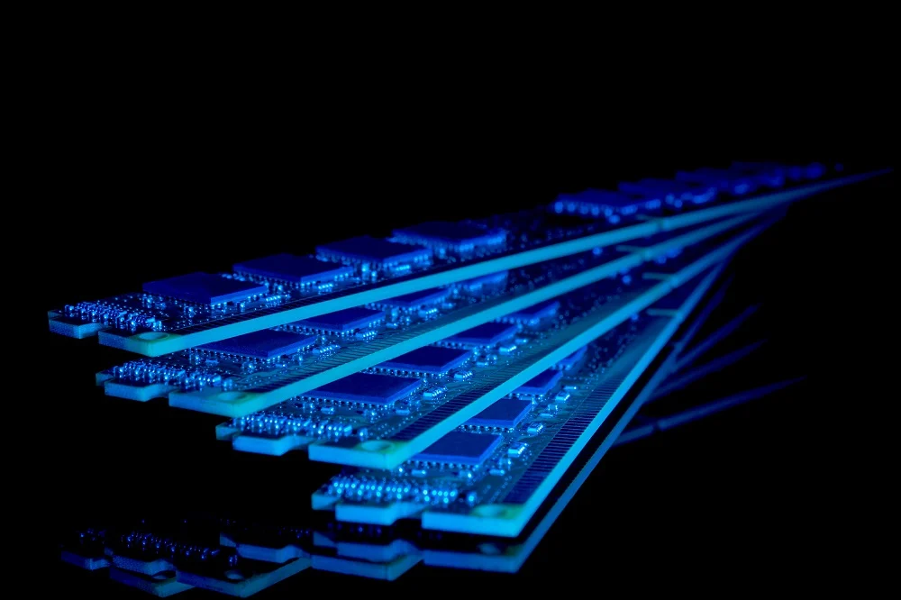
Magnetoresistive Random Access Memory (MRAM)—a technology once relegated to the fringe of semiconductor research—has officially hit a commercial and technical tipping point. As the industry grapples with the limitations of traditional charge-based memories like NAND and DRAM, MRAM has emerged as a frontrunner for the next generation of computing. To capitalize on this momentum, the Storage Networking Industry Association (SNIA) has announced the launch of the MRAM Alliance Special Interest Group (SIG), a collaborative body designed to align the entire semiconductor value chain behind the technology.
The State of the Market: Moving Beyond the Lab
For years, MRAM was viewed as a promising yet perpetually "emerging" technology. Today, that narrative has shifted. Spin-transfer torque (STT) MRAM has been successfully integrated into the production lines of major global foundries, including TSMC, Samsung, UMC, and GlobalFoundries. This transition from experimental fab runs to high-volume manufacturing signifies that the technology is no longer a theoretical curiosity but a stable, reliable component in modern electronics.
Jean-Pierre Nozières, co-chair of the newly formed MRAM Alliance SIG, characterizes the current climate as a rare window of opportunity. During a recent briefing, Nozières emphasized that MRAM’s maturity level has significantly eclipsed that of alternative non-volatile memory (NVM) technologies, such as resistive RAM (ReRAM) or ferroelectric RAM (FeRAM). "We believe there is a window of opportunity for MRAM because it has reached a maturity level which is much higher than what it is today for resistive RAM or ferroelectric RAM," Nozières stated.

A Chronology of Integration and Expansion
The evolution of MRAM has been a long-term play, defined by gradual integration into specific high-value sectors before attempting broad market penetration.
- Initial Research Phase: For decades, MRAM remained in the realm of academic and corporate R&D, focused on the physics of magnetic tunnel junctions (MTJs).
- The Foundational Shift: The adoption of STT-MRAM by major foundries marked the transition to a viable manufacturing process. This provided the necessary reliability metrics required for commercial-grade silicon.
- Vertical Penetration (Automotive and Space): Early adopters in the automotive sector, such as NXP, began replacing NOR flash with embedded MRAM to improve performance and reliability in microcontrollers. Simultaneously, the radiation-hardened nature of MRAM made it an attractive candidate for aerospace applications, where charge-based memory is prone to bit flips caused by cosmic rays.
- Formation of the SIG: Recognizing that technology readiness was no longer the primary barrier, the industry moved to form the MRAM Alliance SIG within SNIA. This group aims to transition MRAM from a specialized niche solution to a mainstream architectural choice.
Addressing the "Elephant in the Room": Magnetic Immunity
Despite its technical superiority in endurance and speed, MRAM faces a significant psychological and engineering hurdle: the perception of magnetic sensitivity. In the industry, this is often referred to as "the elephant in the room."
Consumers and engineers alike have expressed concerns that external magnetic fields—potentially from magnets in headphones, laptop lids, or industrial equipment—could corrupt data stored within MRAM cells. Nozières acknowledges these concerns but maintains that they are largely based on outdated perceptions.

"Most STT-MRAM parts are rated well above typical ambient magnetic exposure," Nozières noted. Modern packaging techniques, including advanced magnetic shielding, ensure that MRAM devices are robust enough to withstand the environments they are likely to encounter. To formalize this, the IEEE is currently developing a standardized approach to magnetic immunity testing. This effort will define the maximum static magnetic field a device can tolerate while maintaining a target bit error rate, providing manufacturers and end-users with the data-driven assurance they need to adopt the technology confidently.
Supporting Data: Why MRAM Matters for AI and Edge Computing
The value proposition of MRAM lies in its unique combination of attributes: it is fast, non-volatile, and possesses nearly infinite write endurance. As we enter the era of ubiquitous AI, these characteristics are becoming mission-critical.
The Memory Bottleneck
Current data center architectures are frequently throttled by the "memory wall"—the latency involved in moving data between storage and processor. By deploying MRAM at the edge, developers can perform inference locally, reducing the reliance on high-latency cloud round-trips.

Performance Metrics
Compared to incumbent technologies, MRAM offers:
- Endurance: While NAND flash degrades after a certain number of write cycles, MRAM can endure trillions of cycles, making it ideal for high-frequency logging and real-time processing.
- Speed: MRAM approaches the speed of SRAM but with the non-volatility of flash.
- Radiation Tolerance: In space-bound systems, MRAM has demonstrated superior immunity to single-event upsets (SEUs) compared to traditional charge-based memories.
Official Responses and Strategic Vision
The formation of the MRAM Alliance SIG is a strategic move to build an ecosystem, not just a product. By operating under the umbrella of the Storage Networking Industry Association (SNIA), the group gains access to a broader cross-section of the market.
"It is very important for us to get end users involved," Nozières said. "SNIA is an organization of end users, not just semiconductor players who understand MRAM’s capabilities."

The SIG’s roadmap includes:
- Education and Communication: Clearing up misconceptions regarding magnetic sensitivity and highlighting the tangible benefits of MRAM over flash and ReRAM.
- Ecosystem Alignment: Bridging the gap between the semiconductor supply chain—foundries, chip designers, and equipment manufacturers—and the companies actually building systems.
- Standardization: While not the immediate focus, Nozières believes that a single JEDEC-like interface standard for MRAM is an inevitable requirement. Standardizing the interface would allow developers to swap MRAM into existing designs as easily as they currently integrate standard DRAM or flash, significantly lowering the barrier to entry.
Implications for the Future of Computing
The push for MRAM comes at a pivotal time in computing history. As AI workloads move from centralized clouds to distributed edge devices, the demand for memory that can survive power cycles without degradation, while remaining fast enough to support real-time processing, has never been higher.
If the MRAM Alliance SIG succeeds, we may see a transition where MRAM moves from being an "alternative" to being a standard component of the memory hierarchy. The goal is to create a plug-and-play reality where MRAM is simply another option on a bill of materials, chosen for its durability and performance rather than avoided due to legacy concerns.

"No technology can be deployed everywhere in every mission profile in every environment," Nozières admitted. However, by fostering a collaborative environment, the MRAM Alliance hopes to ensure that for the millions of applications where MRAM is the optimal fit, the path to implementation is as frictionless as possible. As the industry shifts its focus from raw capacity to endurance and speed, MRAM is positioned to become the quiet workhorse of the next decade of silicon innovation.
Author
Related Posts
Toshiba Unveils High-Performance Multiplexers to Power Next-Generation PCIe 6.0 and USB4 v2 Architectures
- 0
- 1,135 word
In the rapidly evolving landscape of high-speed data interconnects, the bottleneck often lies not in the processor or the memory, but in...
Read out all
DEEPX Unveils the DX-AIPlayer: Bridging the Gap Between Edge Computing and High-Performance AI
- 0
- 1,258 word
In the rapidly evolving landscape of edge artificial intelligence, the demand for hardware that balances power efficiency with high-throughput inference has never...
Read out allThe Smart Shopper’s Pulse: Tracking the Best Daily Deals in an Era of Digital Hype
- 0
- 1,214 word
By Daniel Oropeza | Shopping Editor May 13, 2026 In the modern digital marketplace, the consumer is bombarded with a relentless stream...
Read out all
Bridging the Digital Divide: How Experience AI is Empowering Classrooms in Uzbekistan
- 0
- 1,266 word
In an era defined by the rapid proliferation of artificial intelligence, the global race to ensure digital equity has moved beyond basic...
Read out all
The Mirror in the Machine: Unmasking Algorithmic Bias in the Age of AI
- 0
- 1,266 word
The widespread adoption of artificial intelligence (AI) has been accompanied by a persistent, often unexamined, myth: that algorithms are objective, mathematically neutral...
Read out all
Coding for the Future: Young Innovators Shine at Coolest Projects USA Minnesota
- 0
- 1,396 word
The Science Museum of Minnesota transformed into a vibrant hub of innovation on April 11, as it played host to the second...
Read out all