
- 0
- 1,135 word
In the rapidly evolving landscape of high-speed data interconnects, the bottleneck often lies not in the processor or the memory, but in the signal integrity of the paths that connect them. As the industry transitions toward PCIe 6.0 and USB4 Version 2.0 standards, the physical layer requirements for signal switching have reached unprecedented levels of complexity. Addressing this critical juncture, Toshiba Electronic Devices & Storage Corporation has announced the launch of its new TDS5C212MX and TDS5B212MX—a pair of 2:1 multiplexer/1:2 demultiplexer switches engineered to handle the blistering data rates required by modern enterprise and consumer hardware.
Main Facts: Engineering for the Terabit Era
The new Toshiba switch portfolio is designed specifically to mitigate signal degradation in systems that operate at the extreme edges of current interface specifications. By leveraging Toshiba’s proprietary TarfSOI (Toshiba advanced RF Silicon-on-Insulator) manufacturing process, these devices offer a robust solution for switching high-speed differential signals.
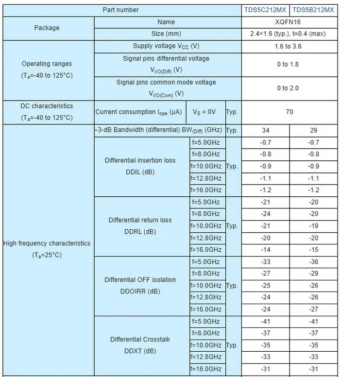
At the heart of these devices are their impressive bandwidth capabilities. The TDS5C212MX boasts a typical differential 3-dB bandwidth of 34 GHz, while its counterpart, the TDS5B212MX, offers a 29 GHz bandwidth. These specifications are not merely academic; they are essential for maintaining signal integrity in environments where even minor waveform distortion can result in significant bit-error rates (BER) and reduced throughput.
These switches are tailored for a diverse array of high-performance applications, including:

- Enterprise Servers: Facilitating high-speed lane switching in data center backplanes.
- Industrial Testers: Ensuring signal fidelity for automated test equipment (ATE) that must validate cutting-edge silicon.
- Robotics: Providing reliable, low-latency communication links for high-precision autonomous systems.
- Consumer PCs: Supporting the latest external interface standards that demand multi-gigabit speeds.
Chronology: The Evolution Toward High-Speed Interconnects
The introduction of the TDS5C212MX and TDS5B212MX follows a multi-year industry trajectory toward increasing bandwidth densities.
Early 2020s: As PCIe 4.0 and 5.0 became mainstream, signal integrity challenges began to dominate the design cycle. Engineers moved away from traditional PCB routing techniques, necessitating specialized signal conditioning and switching components.
2024–2025: The industry saw the formalization and early adoption of PCIe 6.0, which utilizes PAM4 (Pulse Amplitude Modulation 4-level) signaling. This modulation scheme is significantly more sensitive to noise and jitter than the NRZ signaling used in previous generations, forcing component manufacturers to prioritize low-insertion-loss designs.
Mid-2026: Toshiba’s announcement marks a critical milestone in the availability of "off-the-shelf" switching components capable of handling the raw bandwidth requirements of PCIe 6.0 and USB4 v2. The release coincides with the broader industry effort to make these high-speed interfaces accessible in non-bespoke, general-purpose industrial and consumer products.

Supporting Data: Why Bandwidth Matters
In high-speed digital design, the "eye diagram" is the ultimate test of a signal path. As frequencies push toward the 30+ GHz range, the copper traces on a PCB, combined with the switches themselves, act as low-pass filters. If the switch bandwidth is insufficient, the edges of the digital pulses become rounded, closing the eye diagram and making it impossible for the receiver to distinguish between a logic high and a logic low.
Technical Specifications Overview
| Feature | TDS5C212MX | TDS5B212MX |
|---|---|---|
| 3-dB Bandwidth | 34 GHz | 29 GHz |
| Function | 2:1 Mux / 1:2 Demux | 2:1 Mux / 1:2 Demux |
| Interface Support | PCIe 6.0 / USB4 v2.0 | PCIe 6.0 / USB4 v2.0 |
| Manufacturing Process | TarfSOI | TarfSOI |
| Temp Range | -40°C to +125°C | -40°C to +125°C |
The TDS5C212MX stands out for its specialized pin layout, which is engineered specifically to minimize the signal path length. In high-frequency RF design, every millimeter of trace length contributes to signal reflection and impedance mismatch. By optimizing the physical layout, Toshiba has significantly reduced these parasitics, allowing for a cleaner transition of high-speed data. Conversely, the TDS5B212MX maintains a pinout consistent with legacy designs, offering a "drop-in" migration path for engineers who need to upgrade performance without redesigning their entire motherboard footprint.
Official Perspectives: The Value of TarfSOI
Toshiba’s reliance on the TarfSOI process is a strategic decision that underscores the company’s focus on radio-frequency and high-speed signal integrity. The Silicon-on-Insulator (SOI) process is inherently better suited for high-frequency switching than traditional bulk CMOS. By placing the transistor channel on an insulating layer, Toshiba significantly reduces substrate capacitance—the primary culprit behind signal leakage and loss at high frequencies.
In technical briefings, Toshiba engineers have emphasized that the "Tarf" (Toshiba Advanced RF) branding reflects years of refinement in insulating materials and gate-stack engineering. The goal is to provide a "transparent" switch—a component that, in the eyes of the digital signal, simply does not exist, thereby preserving the integrity of the data stream from source to destination.

Implications for Future Design
The implications of this launch are far-reaching for several sectors of the electronics industry.
1. The Death of the "Bottleneck"
For years, the limitation of interface speed was often tied to the physical layer. With switches like the TDS5C212MX, the physical path is no longer the primary hurdle. This allows architects to push for higher clock speeds in PCIe lanes without fearing that the multiplexing logic will become a failure point.
2. Standardized High-Speed Switching
Previously, companies looking to implement custom PCIe 6.0 switching often had to rely on expensive, custom-designed ASICs or complex FPGA-based solutions. Toshiba’s move to make these components available as standard logic ICs democratizes high-speed design, allowing smaller firms to build enterprise-grade hardware at a fraction of the R&D cost.
3. Thermal Reliability in Rugged Environments
The operating range of -40°C to +125°C is significant. PCIe 6.0 and USB4 v2 interfaces are increasingly finding their way into "edge" environments—outside of climate-controlled data centers. Whether it is in a robotic arm operating in a factory or an industrial tester in an unconditioned warehouse, the ability for these components to maintain stable impedance characteristics across a 165-degree temperature delta is critical for long-term product reliability.

Conclusion
As we stand on the precipice of a new era of data density, the underlying hardware must be as resilient as the protocols it supports. Toshiba’s introduction of the TDS5C212MX and TDS5B212MX represents a proactive response to the physical limitations of high-speed signaling. By combining advanced SOI manufacturing with thoughtful, application-specific pin configurations, Toshiba is providing the "glue" that will hold together the next generation of server, industrial, and consumer architectures.
As these devices begin to ship, the industry will watch closely to see how they perform in real-world, high-stress deployments. If the performance metrics hold true under sustained heavy data loads, these switches could quickly become the standard-bearer for high-speed connectivity, setting the bar for what is expected of the humble, yet essential, multiplexer.
For engineers and developers looking to integrate these components, full technical documentation and design support are now available via the official Toshiba Electronic Devices & Storage portal. As the digital world continues to accelerate, Toshiba has ensured that the pathways for that data remain open, clear, and exceptionally fast.
Author

Related Posts
MRAM Reaches a Strategic Tipping Point: New Industry Alliance Formed to Scale Adoption
- 0
- 1,114 word
Magnetoresistive Random Access Memory (MRAM)—a technology once relegated to the fringe of semiconductor research—has officially hit a commercial and technical tipping point....
Read out all
DEEPX Unveils the DX-AIPlayer: Bridging the Gap Between Edge Computing and High-Performance AI
- 0
- 1,258 word
In the rapidly evolving landscape of edge artificial intelligence, the demand for hardware that balances power efficiency with high-throughput inference has never...
Read out all
The Smart Shopper’s Pulse: Tracking the Best Daily Deals in an Era of Digital Hype
- 0
- 1,214 word
By Daniel Oropeza | Shopping Editor May 13, 2026 In the modern digital marketplace, the consumer is bombarded with a relentless stream...
Read out all
Bridging the Digital Divide: How Experience AI is Empowering Classrooms in Uzbekistan
- 0
- 1,266 word
In an era defined by the rapid proliferation of artificial intelligence, the global race to ensure digital equity has moved beyond basic...
Read out all
The Mirror in the Machine: Unmasking Algorithmic Bias in the Age of AI
- 0
- 1,266 word
The widespread adoption of artificial intelligence (AI) has been accompanied by a persistent, often unexamined, myth: that algorithms are objective, mathematically neutral...
Read out all
Coding for the Future: Young Innovators Shine at Coolest Projects USA Minnesota
- 0
- 1,396 word
The Science Museum of Minnesota transformed into a vibrant hub of innovation on April 11, as it played host to the second...
Read out all